What is an IC 4017 Decade Counter?
The IC 4017, also known as a decade counter, is a CMOS (Complementary Metal-Oxide-Semiconductor) integrated circuit primarily used in electronic counting and sequencing applications. Specifically, the IC 4017 is referred to as a "Johnson Decade Counter," and it has the capability to count in a sequence from 0 to 9.
.jpg)
Overview and Features:
- Type: CMOS Decade Counter
- Package: Generally housed in a 16-pin Dual In-line Package (DIP)
- Manufacturer: The IC 4017 is manufactured by various companies including Texas Instruments, STMicroelectronics, and others.
Features and Functionality:
-
Decade Counter: The IC 4017 primarily functions as a 10-stage (decade) counter. It sequentially produces output logic high on one of its 10 output pins based on the current count value.
-
Clock Input: It has a clock input pin (usually "CLK") receiving clock pulses to trigger the advancement of the count.
-
Decoding Logic: The outputs are internally decoded to provide a corresponding logic high on one of the 10 output pins at a time.
-
Reset Pin: It often includes a "Reset" pin that enables resetting the count back to a predefined state.
-
Applications: It is widely used in applications such as frequency dividers, LED chasers, digital clocks, and sequential timing circuits. Additionally, it's often used in combination with other ICs to achieve specific sequencing and timing functions.
Applications:
-
Timing and Sequencing: Often used in applications where specific timing and sequencing are required, such as in digital clocks, sequential LED lighting, and programmable sequential controllers.
-
Frequency Division: Employed as a frequency divider, dividing down higher frequency signals to lower frequency signals.
-
Logic Circuits: Utilized as part of more complex logic circuits for controlling various events and functions.
The IC 4017 is widely used in hobbyist electronic projects, educational purposes, and in some commercial applications due to its ease of use and its ability to provide sequential outputs based on clock pulses. Its straightforward functionality makes it a valuable tool for learning about digital electronics and for creating basic sequential logic circuits.
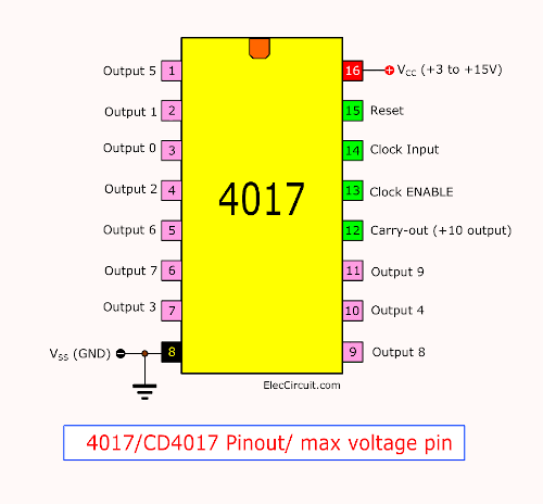
CD4017 Pinout
The CD4017 is a CMOS integrated circuit (IC) called a "Johnson Decade Counter." Its pinout and functionality are crucial to understanding its application. Here's the pinout of the CD4017:
.jpg)
Pin Configuration:
The CD4017 typically comes in a 16-pin Dual In-line Package (DIP). Here are the functions of its pins:
-
Pin 1 (MR, Master Reset): This pin is used to reset the count to zero when it receives a high (logic 1) signal. It overrides all other inputs. When this pin is connected to the supply voltage, the count is reset.
-
Pin 2 (CLOCK, Clock Input): This is the clock input pin. When a positive clock edge is detected (i.e., a rising edge), it advances the count by one. The count advances on each clock pulse.
-
Pin 3 (Q0 - Q4): These are the decoded output pins. They represent the count values 1 through 10 (as it's a decade counter), with the count resetting at Q0.
-
Pin 4 (Q5, Carry Out): This pin goes high (logic 1) if the count reaches 5 (or any other predefined count) and provides a carry-out signal, allowing cascading to another counter or device.
-
Pins 5 and 10 (DEC, DECADE and ENABLE, respectively): These pins handle the reset and enabling functions for cascading multiple CD4017 ICs.
-
Pins 6 and 7 (Q6 and Q7): These are the additional decoded output pins. When used along with the other outputs, these pins can create more complex counting sequences.
-
Pin 8 (GND): This is the ground (0V) pin, providing the reference voltage for the IC's operation.
-
Pin 9 (CARRY IN): This pin allows cascading multiple CD4017 counters together. When the count reaches the maximum (10 in the case of CD4017), this carry-in signal can reset the counting or trigger other logic.
-
Pin 11 (CLOCK INHIBIT): When this pin is held high (logic 1), clock pulses are ignored, inhibiting counting.
-
Pin 12 (Q5): A duplicate of the Q5 output pin.
-
Pin 13 (STROBE): This pin is used for clocking the IC with a 2-phase clock (dual input clock).
-
Pin 14 (CLOCK ENABLE): When this pin is connected to the supply voltage, it enables the clock input; otherwise, the clock input is ignored.
-
Pin 15 (VDD or VCC): This is the positive power supply pin for the IC, typically connected to a +5V or other suitable supply voltage.
-
Pin 16 (VDD or VCC): Another positive power supply pin, similar to pin 15, providing the required supply voltage for the IC's operation.
Understanding the pinout and functionality of the CD4017 is essential for effectively using this IC in various electronic projects, especially those involving digital logic, sequencing, and counting applications.
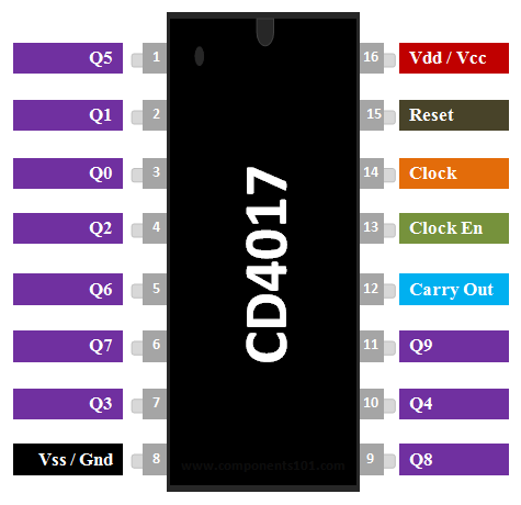
CD4017 IC Features
The CD4017 is a CMOS integrated circuit primarily used as a 10-stage Johnson decade counter and divider. Known for its versatility and simplicity, it offers several features that make it a popular choice in a wide array of electronics applications. Here are its key features:
Key Features of the CD4017 IC:
-
Decade Counter Operation: The CD4017 operates as a 10-stage counter, meaning it can sequence through 10 different states or outputs.
-
CMOS Technology: Built using CMOS technology, the IC offers low power consumption alongside a wide supply voltage range.
-
Clock Input: The CD4017 features a clock input (pin 14) that triggers the advancement to the next state with each clock pulse.
-
Decoded Outputs: The 10 decoded outputs (Q0 to Q9) are used to indicate the current count state.
-
Carry Output: It includes a carry-out (CO) pin (pin 12) that generates a pulse when the count exceeds 9, allowing for cascading with other ICs.
-
Reset Functionality: The IC includes a reset pin (MR, pin 15) that can reset the counter and outputs to 0 when triggered.
-
Enable and Inhibit Pins: It offers pins for enabling clock inputs (pin 13) and inhibiting clock pulses (pin 11).
-
Multiple Power Supply Pins: The IC has multiple VDD or VCC pins (pins 8 and 16) for easy integration with power supplies.
-
Built-in Decoding Logic: The IC integrates decoding logic to facilitate straightforward usage, allowing each output to represent a specific count state.
-
Wide Operating Voltage Range: It operates within a wide voltage range, typically ranging from 3V to 15V, providing great flexibility in various applications.
-
Compact form factor: The CD4017 comes in the standard 16-pin DIP (Dual In-line Package) format, ensuring compatibility with conventional breadboards and PCBs.
Applications:
The CD4017's features make it suitable for various applications:
-
Sequential Lighting: It is widely used in LED chaser and sequential lighting circuits due to its ability to sequence through its outputs.
-
Digital Timers and Clocks: Its 10-stage counting ability makes it suitable for timer and clock applications which require counting in seconds, minutes, or hours.
-
Frequency Dividers: The IC can function as a frequency divider, dividing the input frequency by 10.
-
Sequencing and Automation: Its counting ability is used for controlling sequenced events, making it ideal for automation and control systems.
-
Educational Purposes: It is also commonly employed in educational settings for teaching digital logic, counting, and sequencing concepts.
The CD4017's features and versatility make it a popular choice in hobbyist projects, educational demonstrations, and various digital sequencing applications due to its simple operation and ubiquitous availability.
Where to Use IC CD4017?
The IC CD4017, a member of the CMOS 4000 series, has a wide range of applications thanks to its ability to count and sequence through ten different states. Here are some common areas where the CD4017 is used:
-
Sequential LED Lighting: One of the most popular uses of the CD4017 is in sequential LED lighting applications, such as decorative lighting, advertising displays, or even in lighting effects for art projects. The IC can cycle through its outputs, effectively and easily controlling the sequencing of different LEDs.
-
Digital Timing and Control: The CD4017 can also be utilized in digital clock and timer circuits, where sequential time-based events are triggered through its outputs. This makes it a key component in digital clock designs, countdown timers, and other time-based control circuitry.
-
Frequency Dividers: This IC can function as a frequency divider, used to divide an input frequency by 10. This is valuable in applications where a lower frequency is required for various operations, such as timing circuits or clock generation.
-
Automated Control Systems: Due to its ability to sequence through states, the CD4017 is utilized in automated control systems, particularly in systems requiring sequential operations or event triggering.
-
Educational Projects: The CD4017 is an excellent educational tool, commonly used in electronics and digital logic courses to teach counting and sequencing concepts. It is often a primary component in student projects to create simple digital circuits.
-
Music and Sound Generation: In combination with other components, the IC can be used to create simple music or sound generation circuits where different tones are produced sequentially.
-
Game Controllers and Toy Circuits: Its ability to control the sequencing and triggering of various events makes the CD4017 an ideal candidate for use in game controllers and toy circuits where sequential operations are required.
-
Industrial Automation and Sequencing: The IC is employed in industrial applications for its ability to trigger operations in a specific sequence, providing straightforward control for various devices and processes.
-
Traffic Light Controllers: It is used in small-scale traffic light control systems for educational purposes or model traffic light demonstrations due to its sequential operation capabilities.
-
Automotive DIY Projects: In automotive projects and DIY circuits, the CD4017 can be used for creating sequential lighting effects in cars or in simple automation systems.
These applications showcase the flexibility and utility of the CD4017 IC in numerous digital and analog electronic projects. Its simple functionality and ability to sequence output states make it a popular and adaptable component in many different electronic systems and devices.
Timing Diagram
The timing diagram of the CD4017, known as the "Johnson Decade Counter," illustrates the sequential output states of the IC in response to clock pulses. It showcases the progression of the output states as the input clock signal triggers the counter. Here's a simplified timing diagram for the CD4017:
-
Input Signal (Clock Signal): The timing diagram begins with the representation of the clock pulses, typically denoted by regular square wave pulses with rising edges triggering the counter.
-
Output States (Q0 - Q9): Following the clock pulses, the timing diagram illustrates the sequential changes in the outputs (Q0 to Q9) of the CD4017 as the counter advances in response to each clock pulse. Each output represents a specific count state, starting from Q0 and progressing up to Q9 before resetting back to Q0.
-
Carry Out (Q5): Additionally, if cascade functionality is used, the timing diagram can depict the carry-out (Q5) signal, which indicates when the count reaches its maximum value (5 in the case of CD4017). This signal can be used to trigger further circuitry or to cascade with another CD4017 for extended counting capabilities.
-
Clear/Reset Signals: In some timing diagrams, you might also find representations of the master reset (MR) signal, showing how it resets the counter to the initial count state (Q0) when activated.
-
Clock Inhibit and Other Control Signals: If additional control signals such as clock inhibit are used in a specific application, the timing diagram might include these signals to demonstrate their effect on the counter's operation.
These signals collectively provide a visual representation of how the CD4017 responds to the clock signal and progresses through its output states. By studying this timing diagram, engineers and designers can better understand the behavior and sequencing of the CD4017 and use this information to integrate the IC effectively into various electronic circuits, timing applications, and control systems.
Working of CD4017 Circuit
The CD4017 is a CMOS integrated circuit commonly used as a 10-stage Johnson decade counter and it finds use in various digital and analog electronic applications. Understanding its basic working principle is important in designing circuits that utilize this IC.
Working Principle:
-
Clock Input (Pin 14): The CD4017 IC functions based on clock pulses. When a clock pulse is applied to its clock input (Pin 14), it activates the counter to advance to the next output stage. The IC recognizes the rising edge of the clock pulse to trigger the count.
-
Output States (Q0 - Q9) and Reset: As the clock pulse is applied, the IC sequentially advances through its ten output states, represented by pins Q0 through Q9. On each rising edge of the clock pulse, the output changes to the next stage in the sequence.
-
Decoding and Output Logic: The IC features built-in decoding logic which activates the outputs in a predetermined sequence. Each output represents a specific count state during the counting process.
-
Carry-Out (CO) Signal (Pin 12): When the count reaches its maximum value (Q9) and another clock pulse is received, a carry-out signal is generated on the CO pin (Pin 12). This carry-out can be used for cascading with other CD4017 ICs or can trigger external circuitry or devices.
-
Reset Functionality (MR, Pin 15): The Master Reset pin (Pin 15) can be used to reset the count back to its initial state (Q0) when pulled high (logic 1). This helps in resetting the count to the starting point as required in various applications.
Example Application - Sequential LED Lighting:
To understand the working principle with an application, let's consider the use of the CD4017 in a sequential LED lighting circuit:
- The CD4017 can be used to sequentially light up a series of LEDs, creating a chasing or scanning effect.
- The clock input is driven by a clock signal (e.g., a 555 timer IC generating a square wave), and the outputs (Q0 - Q9) are connected to individual LEDs.
- As each clock pulse is received, the IC advances to the next output, lighting up the corresponding LED in the sequence.
- When the count reaches the maximum state, the carry-out signal can be used to trigger the reset of the counter or to cascade to another CD4017 IC for extended sequencing.
This simple example illustrates the basic working principle of the CD4017 as a sequential counter in a practical application.
It's important to note that while the concept is straightforward, proper current limiting resistors and considerations for current sourcing capabilities should be taken into account when using the CD4017 to drive LEDs or other loads. Additionally, timing considerations, clock frequencies, and sequencing configurations can significantly impact the overall performance and behavior of the circuit.
.jpg)
Working Principle of CD4017
The CD4017 is a versatile CMOS-based integrated circuit known as a "Johnson Decade Counter." Its working principle is fundamental to understanding its function in numerous electronic applications. Here's a breakdown of its working principle:
Clock Input and Output Sequence:
-
Clock Signal Reception: The CD4017 IC operates by responding to a clock signal applied to its clock input (Pin 14). When a clock pulse is received at the clock input, the IC advances its internal state by one. It typically recognizes the rising edge of the clock signal to trigger the counting operation.
-
Output Sequence: As the CD4017 receives clock pulses, it cycles through its ten output states sequentially. Each output state (Q0 to Q9) corresponds to a specific count value, progressing from 0 to 9 in a continuous loop. For example, the Q0 output goes high with the first clock pulse, while the Q9 output goes high after the ninth clock pulse, and then resets to Q0 after the tenth pulse.
Decoding and Output Logic:
-
Decoding Logic: Internal decoding logic in the CD4017 interprets the count value and activates the corresponding output pin.
-
Output Activation: As the CD4017 counts, only one output (from Q0 to Q9) is active at any given time, indicating the current count state. This enables the IC to effectively represent the count in a sequence.
Carry-Out Signal and Reset Functionality:
-
Carry-Out (CO) Signal: When the count reaches 9 (Q9) and another clock pulse is received, the CD4017 generates a carry-out signal on the CO pin (Pin 12). This signal can be used for external cascading of multiple CD4017 ICs to extend the counting sequence or activate external circuitry.
-
Reset Functionality: The CD4017 includes a reset pin (MR, Pin 15) to reset the count back to the initial state (Q0). When the reset input is activated, the count is set back to the beginning of the sequence.
Applications of the Count States:
The count states provided by the CD4017 can be used to trigger or control various events in a wide range of applications, such as LED sequencing, digital timers, frequency dividers, and more. The IC's ability to represent count states in a sequence makes it a valuable component in numerous digital and analog circuits.
In summary, the CD4017's working principle relies on clock signals to cycle through its ten output states in a defined sequence, with built-in decoding logic activating specific output pins to represent the current count value. This functionality makes it an essential component in various electronic projects ranging from simple LED chasers to complex control systems.
Working Process of CD4017
The CD4017, a CMOS-based integrated circuit, operates as a 10-stage Johnson decade counter and is used in a variety of digital and analog applications. Understanding its working process is essential to comprehend its function in electronic circuits. Here is an overview of its working process:
Basis of Operation:
-
Clock Signal Reception: The CD4017 functions by responding to clock signals applied to its clock input (Pin 14). Each rising edge of the clock signal causes the IC to advance to the next output stage.
-
Output Sequence: The IC has 10 output pins labelled Q0 through Q9, and one output goes high at a time in a predetermined sequence as the clock input receives pulses. Each output represents a count value from 0 to 9. As the clock pulses are received, the outputs cycle through the sequence repeatedly.
Decoding and Logic:
-
Output Activation: As the CD4017 counts, one output becomes active at a time in a sequence allowing for the representation of the current count state.
-
Internal Decoding Logic: The IC has built-in decoding logic that enables the activation of the outputs in the correct sequence. This simplifies the process of directing the count progression as well as connecting the outputs to external components.
Reset and Carry-Out Functionality:
-
Carry-Out (CO) Signal: Upon reaching the 10th count (Q9), the CD4017 generates a carry-out signal (Pin 12). This signal can be used to trigger external circuitry or to cascade with additional CD4017 ICs for extended counting sequences.
-
Master Reset (MR, Pin 15): The CD4017 includes a master reset pin. When a high signal is applied to this pin, it resets the count back to the initial state, typically Q0, effectively restarting the sequence.
Utilizing Count States:
The count states provided by the CD4017 can trigger various events or control different elements within a circuit. These count states are easily interpreted and utilized in a wide range of applications, varying from simple LED chasers to complex digital automation systems.
In summary, the CD4017's working process revolves around the reception of clock signals, cycling through its ten output states in a predefined sequence, and utilizing built-in decoding logic to activate specific output pins representing the current count value. This functionality renders it an invaluable component in numerous electronic projects, especially those that require sequencing, counting, or control operations.
.jpg)
How To Use The CD4017 IC?
Using the CD4017 IC involves understanding its pin configuration, connecting it to power, providing a clock signal, and utilizing its outputs to control external components. Here's a detailed guide on how to use the CD4017 IC in a simple LED sequencing circuit:
Required Components:
- CD4017 IC
- LEDs
- Resistors (for current limiting)
- Power supply (Vcc and Ground)
- Clock signal (from a 555 timer, microcontroller, or any other suitable source)
- Breadboard and jumper wires
Steps to Use the CD4017 IC:
-
Understanding the Pinout:
- Pin 16 (Vdd): Connect to the positive power supply (Vcc).
- Pin 8 (GND): Connect to the ground (0V) of the power supply.
- Pin 14 (Clock Input): Connect the clock signal source to this pin.
- Pins 3, 2, 4, 7, 10, 1, 5, 6, 9, 11 (Q0 - Q9): Connect these pins to the components or devices you want to control or sequence (in this case, LEDs).
- Pin 12 (Carry Out): This pin can be used for cascading with additional CD4017 ICs or for triggering external components.
- Pin 15 (Reset): This pin can be used to reset the count back to the initial state.
-
Connecting LEDs:
- Connect the anodes of the LEDs to individual output pins (Q0 - Q9) through current-limiting resistors (appropriate for the specific LEDs being used).
- Connect the cathodes of the LEDs to the ground (0V) of the power supply.
-
Power Supply:
- Connect the Vdd (Pin 16) to the positive terminal of the power supply (Vcc).
- Connect the GND (Pin 8) to the negative terminal of the power supply (ground, 0V).
-
Clock Signal:
- Connect the clock input (Pin 14) to the output of your clock signal source, such as a 555 timer or a microcontroller generating a suitable clock signal.
-
Master Reset (Optional):
- Connect a toggle switch or a push-button to the Reset pin (Pin 15) if you want to manually reset the count back to the initial state.
-
Testing and Operation:
- Apply power to the Vcc and ground pins of the CD4017 IC.
- Apply the clock signal to the clock input (Pin 14).
- As the clock pulses are applied, the outputs of the CD4017 will cycle through their states, lighting up the connected LEDs sequentially.
Keep in mind the current limitations of the CD4017 IC. If you're driving devices that require more current than the IC can safely provide, you might need to use additional components such as transistors or optocouplers for driving larger loads.
Safety Precautions:
- Always ensure correct polarity when connecting power supply and components.
- Be mindful of current limitations and ensure proper current limiting for LEDs or other components.
By following these steps, you can set up a simple LED sequencing circuit using the CD4017 IC. This approach can be extended to control other components or devices, enabling a wide range of applications such as digital control, sequencing, and timing.
How to Cascade the IC 4017 Counter
Cascading IC 4017 counters can be a useful technique in various sequential applications, enabling the creation of larger counting sequences. Cascading multiple IC 4017 counters essentially allows for the expansion of the counting range beyond the ten output stages of a single IC.
Cascading IC 4017 counters involves connecting the output of one IC 4017 to the input of another, which extends the counting sequence further. Here's a general overview of how to cascade IC 4017 counters:
Cascading Two IC 4017 Counters:
-
Connect the Clock Signal:
- Provide the same clock signal to the clock input (Pin 14) of both ICs. This ensures that both counters advance simultaneously.
-
Connect Output to Input:
- Take the carry-out pin of the first IC 4017 (Pin 12) and connect it to the clock input (Pin 14) of the second IC 4017. This feedforward connection essentially enables the second IC to advance its count once the first IC completes its count and triggers the carry-out signal.
-
Reset Signal (Optional):
- If you want to reset the entire cascaded sequence, apply a common reset signal to the reset pins (Pin 15) of both ICs.
-
Output Utilization:
- Utilize the outputs of both ICs as needed to control different sequential tasks or to drive different outputs based on the extended count sequence.
Example Cascaded Counting Sequence:
- With two cascaded CD4017s, you can create a counting sequence from 0 to 99 instead of just 0 to 9. The first CD4017 will count from 0 to 9 and then trigger the second CD4017 to advance, effectively creating a two-digit counter.
Considerations:
-
Clock Timing: Ensure that the clock signal is appropriately timed for the combined counting range. If the clock pulses are very fast, the cascaded sequence can become challenging to manage. Conversely, if the clock pulses are too slow, the sequence may not function as expected.
-
Reset Handling: When employing a reset signal, ensure that it resets both counters simultaneously to avoid any inconsistencies within the cascaded sequence.
-
Output Utilization: The extended count can be utilized to control more complex tasks or to drive multiple outputs in sequence, providing a wider range of applications for sequential control.
By following these steps, you can cascade the IC 4017 counters to create extended counting sequences for a variety of electronic projects, thereby expanding the utility and capacity of the CD4017 for sequential control and counting applications.
CD4017 Application Circuit
The CD4017 is a versatile integrated circuit commonly used for various digital applications. One of the most common applications of the CD4017 is as a decade counter/divider. Additionally, it is often used in sequential circuits, LED chasers, frequency dividers, and more. Below, I'll describe a basic application circuit for the CD4017 using LED sequencing as an example.
LED Sequencing with a CD4017:
Requirements:
- CD4017 IC
- LEDs (any color as per preference)
- Resistors for current limiting on the LEDs
- Power supply (5V is commonly used, as CD4017 works within a range of 3V to 15V)
Circuit Description:
In this application, we are using the CD4017 to sequentially light up an array of LEDs, resulting in a simple LED chaser circuit.
Circuit Diagram:
Circuit Working:
- Connect Pin 16 (VDD) of the CD4017 to the positive terminal of a 5V power supply.
- Connect Pin 8 (GND) of the CD4017 to the negative terminal of the power supply (ground).
- Connect a 10k resistor between Pin 16 and Pin 8 to pull the reset pin (Pin 15) low (it is a good practice to keep it low for proper functioning).
- Connect LEDs in series with current-limiting resistors between Pin 3 (Q0) and Pin 7 (Q4) of the CD4017.
Operation:
- As the clock signal pulses the Clock input (Pin 14), the CD4017 advances through its output states, lighting up the LEDs one after the other.
- Once Pin 7 (Q4) is activated, it resets back to Pin 3 (Q0), and the cycle repeats, creating a sequencing LED chaser effect.
Notes:
- The current-limiting resistors are essential to ensure that the LEDs are not damaged by excessive current.
- The sequencing speed can be adjusted by modifying the clock input signal frequency.
This application demonstrates a basic LED chaser circuit using the CD4017, allowing for a clear visual representation of the IC's sequential counting ability. Keep in mind that this is just one of many possible applications for the CD4017, and this versatile IC can be utilized in a wide range of other digital and sequential control circuits.
Advanced Circuit Design Projects with CD4017
The CD4017 is a versatile IC that can be used in a variety of advanced circuit design projects. Here are a few advanced circuit design applications utilizing the CD4017:
1. Music Sequencer:
Utilize the CD4017 to create a music sequencer. Each output of the CD4017 can trigger a sound module or control voltage for a synthesizer. By connecting the CD4017 outputs to a digital-to-analog converter (DAC), you can control the pitch, duration, and volume of different musical notes.
2. Traffic Light Controller:
Design a traffic light controller using the CD4017. The outputs of the CD4017 can be used to control the red, yellow, and green LEDs representing the lights of a traffic signal. Incorporate timing components to create realistic traffic light sequencing.
3. Combination Lock:
Implement a combination lock using the CD4017. Each digit of the combination can correspond to one of the outputs of the CD4017. When the correct combination is input, a solenoid or motor can be activated to unlock a door or a safe.
4. Digital Dice:
Create a digital dice circuit utilizing the CD4017. When a button is pressed, the CD4017 can be used to produce a random number output by lighting up one of six LEDs—mimicking the rolling of a dice. This can be a fun electronic project for educational purposes.
5. Sequential LED Matrix Display:
Construct a sequential LED matrix display with the CD4017. By using multiple CD4017 ICs cascaded together, you can control the rows and columns of an LED matrix to create scrolling text, patterns, or simple animations.
6. Electronic Quiz Buzzer System:
Develop an electronic quiz buzzer system using the CD4017 to control player response buttons. Each output of the CD4017 can be associated with a player's buzzer, and an associated logic circuit can determine and display the first player to respond by lighting a corresponding indicator.
7. Arduino or Microcontroller Interaction:
Integrate the CD4017 with an Arduino or other microcontroller to create advanced effects and responses. Utilize the CD4017 for generating specific events in response to input or as part of a larger control system.
For each of these projects, make sure to thoroughly understand the operating parameters of the CD4017, including its clock input, output states, and cascading capabilities. Additionally, review safety considerations, such as current limitations, when designing and implementing these circuits.
CD4017 Equivalent IC
The CD4017 is a popular CMOS integrated circuit used as a decade counter and is widely available. However, there are equivalents to the CD4017 that can be used interchangeably in many circuit applications. One such equivalent is the HEF4017.
The HEF4017 is functionally similar to the CD4017 and is also a CMOS-based decade counter/divider. While both the CD4017 and HEF4017 have matching pinouts and functionalities, slight differences might exist in their electrical specifications such as operating voltage ranges and input capacitances.
When replacing a CD4017 with an equivalent such as the HEF4017 or any other compatible IC, it's important to consult the datasheets of both ICs to ensure compatibility for a specific application.
CD4017 Applications
The CD4017, a versatile CMOS integrated circuit, can be used in various applications due to its ability to count and sequence through 10 different states. Here are a few common applications of the CD4017 IC:
1. LED Chaser or Sequential LED Lighting:
The CD4017 is commonly used to create LED chaser circuits where LEDs light up in sequence. This is often seen in decorative lighting, advertising displays, or as eye-catching visual effects, and it's a popular project for hobbyists and students due to its relative simplicity.
2. Digital Timers and Clocks:
The CD4017's ability to sequentially count through its outputs makes it ideal for digital timer and clock circuits. This is useful for creating countdown timers, clock displays, or any application where sequential timing is required.
3. Frequency Dividers:
The IC is used to divide the input frequency by 10, making it valuable in applications where a lower frequency is needed for various operations, such as in timing circuits or clock generation systems.
4. Sequential Control Applications:
The IC is used in applications where events need to be triggered in a specific sequence. It is suitable for controlling sequences in automated systems, such as in industrial control systems, vending machines, or sequential processing equipment.
5. Educational Labs and Demonstrations:
In educational settings for electronics and digital logic courses, the CD4017 is commonly used to teach counting and sequencing concepts. It's also a crucial component in student projects for creating simple digital circuits.
6. Toy and Game Circuits:
Due to its sequential operation capabilities, the CD4017 is used in game controllers, toys, and hobbyist projects where sequential actions or events are required.
7. Traffic Light Controllers (Educational and Small Scale):
In educational settings or small-scale model setups, the IC is used to simulate traffic light control systems to demonstrate sequential operation and simple control systems.
8. Automotive DIY Projects:
In automotive projects and DIY circuits, the CD4017 can be used in creating sequential lighting effects or simple automation systems, such as turn signal sequencing or decorative lighting.
9. Music and Sound Generation:
In combination with additional circuitry, the CD4017 can be used to generate simple music or sound effects by controlling the sequential activation of sound-producing elements.
10. Industrial Automation:
In various industrial settings, the CD4017 can be used for its sequence control capability, facilitating the timed activation of different components in machines and manufacturing processes.
The CD4017's simplicity, versatility, and ability to control sequential events make it a popular choice for a wide range of electronics applications, especially in educational, hobbyist, and small-scale industrial projects.
CD4017 Datasheet
I can't provide a direct link to the CD4017 datasheet as I don't have the capability to browse the internet or provide real-time content from external sources. However, you can easily find the CD4017 datasheet by performing a simple web search using the IC's full name "CD4017 datasheet." The datasheet will typically be available from the manufacturer’s website or from various electronics component distributors. It is important to ensure that you are obtaining the datasheet from a reliable and official source.
The datasheet contains comprehensive information about the CD4017, including its pinout, electrical characteristics, functional description, application information, and much more. It serves as a critical reference when working with the CD4017 IC in electronic circuit design or troubleshooting.
When reviewing the datasheet, pay special attention to the electrical specifications, recommended operating conditions, timing diagrams, and application examples to understand how to effectively implement the CD4017 in your circuit designs.
Conclude
In conclusion, to access the specific CD4017 datasheet, I recommend conducting a web search using the term "CD4017 datasheet." This search will yield results from various trustworthy sources, including the manufacturer's official website and respected electronics component distributors. The datasheet is an essential resource, offering detailed information about the CD4017 integrated circuit, including pin configurations, electrical characteristics, functional descriptions, timing diagrams, and application guidelines. Accessing the official datasheet will provide you with the necessary details to effectively integrate the CD4017 into your electronic circuit designs and applications.
Read More
I don't have direct browsing capabilities to fetch real-time data or access external websites to provide the latest or specific datasheets. However, you can easily find the CD4017 datasheet by doing a simple web search using the term "CD4017 datasheet." This search will provide you with access to the datasheet from various reliable sources, including the manufacturer's official website, electronics component distributors, or trusted electronic component databases. These datasheets offer comprehensive details to help you effectively utilize the CD4017 integrated circuit in your electronic designs and projects.